
ESE101: Microcontroller Peripherals, GPIOs, and Blinking Lights Part 2
Now that I've explained what peripheral control registers look like at a high level, let’s see what the GPIO control registers are like.
The MSP430 has a number of bits to control each GPIO pin. The three most important control bits are:
Direction: The direction bit configures the GPIO as an input or output.
Output: If the GPIO is configured as an output, the output bit sets the GPIO pin to be either 0 or 1. Normally a GPIO can be either 0 or 1 (low or high voltage).
Input: If the GPIO is configured as an input, reading the input bit will tell you if the voltage on the GPIO pin is 0 or 1 (low or high voltage).
If you remember, the datasheet entry said this about GPIO P1:

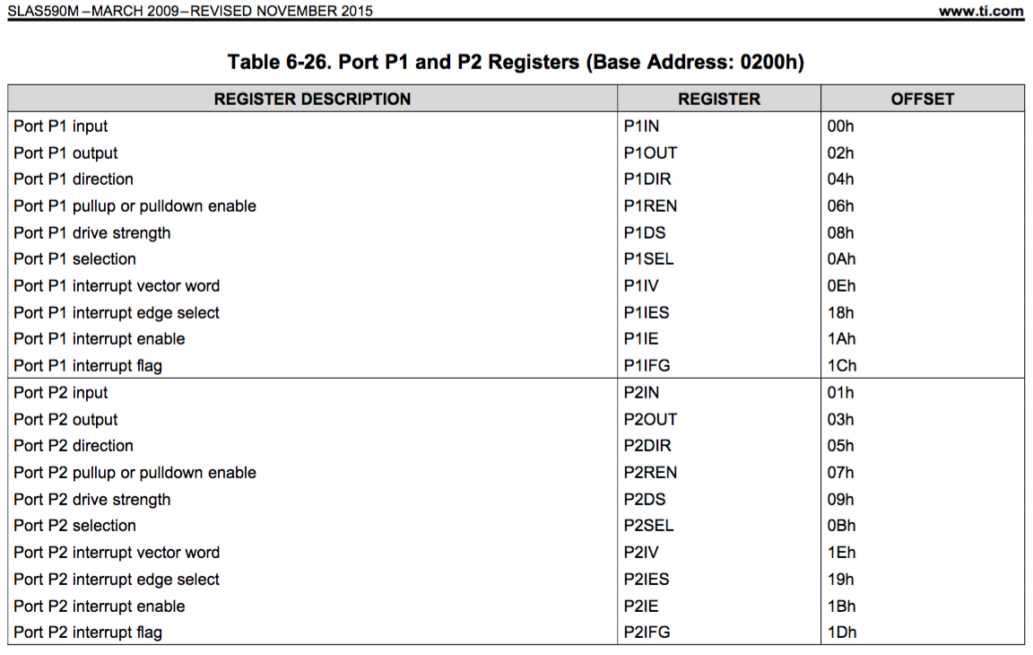
Let’s do as it suggests and see Table 6-26 for more details:
Okay, now we’re getting somewhere.
This table tells us that Port P1 control registers are at the even offsets starting at 0x0200:
Port P1 input (P1IN): 0x0200 (0x0200 + 0x00)
Port P1 output (P1OUT): 0x0202 (0x0200 + 0x02)
Port P1 direction (P1DIR): 0x0204 (0x0200 + 0x04)
Etc.
And Port P2 has the odd offsets (P2IN is at 0x0201, P2OUT is at 0x0203, etc.).
Each register is 8-bits wide, and each bit corresponds to one GPIO pin. So P1IN bit 0 corresponds to Port 1 pin 0, bit 1 corresponds to Port 1 pin 1, and so on.
Note that the P1 and P2 registers are interleaved: P1IN is followed by P2IN, then P1OUT is followed by P2OUT, and so on.
Let’s fill in the drawing of the control registers with the actual control registers names:

Note that the last two addresses 0x021E and 0x021F aren’t assigned to anything in Table 6-26. I’m not sure what would happen if an instruction tried to read or write 0x021E or 0x21F. Maybe nothing would happen, or maybe it would cause a chip error? Microcontrollers have plenty of these undefined memory locations; I just ignore them.
Hopefully now you understand what a peripheral and GPIO are and how a microcontroller uses memory mapped registers to control them.
So how do we actually use these GPIO control registers? Tune in to Part 3 next week to find out!
(You can check out chapter 12, “Digital I/O Module,” in the MSP430’s User Guide if you can’t wait until next week!)
This post is part of a series. Check out the complete Embedded Software Engineering 101 series here.